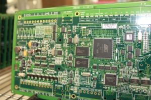
 The spacing of components on PCBs is both art and science. As densities increase and designers strive to meet demands for more compact devices, they must make trade-off decisions that affect yield and may risk potential manufacturing problems.
At OCM Manufacturing, we like to work with our customers to make the best possible trade-offs in the design. This DFM Tip provides general guidelines for optimizing component spacing on both surface mount and pin through-hole circuit boards.
Compact Spacing: The Trade-Offs
A variety of goals may drive the requirement for high-density designs, including small form factor applications and pressure to reduce materials costs. However, the manufacturing repercussions of high-density designs can quickly escalate costs. For example:
- If rework is required, tightly packed components typically add additional time and costs – heat shield may need to be added and additional components may need to be removed to access others.
- Placement machines may need to be reprogrammed to prevent interference with nozzles that may arise when tall components are placed adjacent to lower components.
- Automated optical inspection (AOI) becomes more challenging when components block each other visually, or cast shadows on one another, and reprograming or a higher number of photographs may be required.
With that said, there are no hard and fast rules for component spacing. Tightly packed components may have very good yield and problems may arise only during rework. We promote awareness and like to work with our customers’ design teams to understand the risks and make the best trade-offs.
Making Optimal Trade-Offs
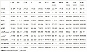
The spacing requirements for every component are unique. The IPC document IPC-7351 (Generic Requirements for Surface Mount Design and Land Pattern Standard) is not straight forward in regards to spacing between components of different packages. We often provide our customers with the spacing chart below.
But for designers who are pushing boundaries of density and who need to take risks that fall outside of standard spacing, we’d prefer to work collaboratively so that they can make the most informed decisions on the trade-offs. For example, we may recommend:
- Rearrangement of components.
- Pushing density in lower cost/lower risk areas of the design and shifting the risk away from higher-risk design areas, such as BGAs, where rework is already costly.
- We can always find solutions – but the optimal time to do so is during layout phase, rather than after agency approvals or customer acceptance milestones have past.
Standard Spacing Chart
This chart  provides best practises for component spacing. Match each component in the rows with whatever it’s adjacent to in the columns to see the preferred and minimum spacing between those two components, in mils.
Spacing values listed in the chart below are for either “pad to pad spacing”, “body to body spacing”, or “body to pad spacing” depending on the orientations of the adjacent parts on the board. The minimum spacing is always between the outside of the perimeter pad if the part body does not overhang that pad. If the part overhangs, then the spacing is from the worst case outside of the body with the pin entirely still on the land.
This covers most cases. We like to review a layout after placement and can then provide the best DFM feedback at that point.
At OCM Manufacturing, we can work with designers to ensure that their plans and prototypes are manufacturable and therefore marketable. Contact one of our Program Managers for details about how we can help.

